The first step towards a final destination – to develop a micro-scale camera for microrobots – Innovation Toronto

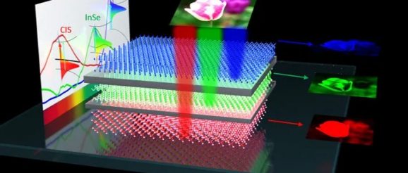
Georgia State University researchers have successfully designed a new type of artificial vision device that incorporates a novel vertical stacking architecture and allows for greater depth of color recognition and scalability on a micro-level. The new research is published in the top journal ACS Nano.
“This work is the first step toward our final destination–to develop a micro-scale camera for microrobots,” says assistant professor of Physics Sidong Lei, who led the research. “We illustrate the fundamental principle and feasibility to construct this new type of image sensor with emphasis on miniaturization.”
Lei’s team was able to lay the groundwork for the biomimetic artificial vision device, which uses synthetic methods to mimic biochemical processes, using nanotechnology.
“It is well-known that more than 80 percent of the information is captured by vision in research, industry, medication, and our daily life,” he says. “The ultimate purpose of our research is to develop a micro-scale camera for microrobots that can enter narrow spaces that are intangible by current means, and open up new horizons in medical diagnosis, environmental study, manufacturing, archaeology, and more.”
This biomimetic “electric eye” advances color recognition, the most critical vision function, which is missed in the current research due to the difficulty of downscaling the prevailing color sensing devices. Conventional color sensors typically adopt a lateral color sensing channel layout and consume a large amount of physical space and offer less accurate color detection.
Researchers developed the unique stacking technique which offers a novel approach to the hardware design. He says the van der Waals semiconductor-empowered vertical color sensing structure offers precise color recognition capability which can simplify the design of the optical lens system for the downscaling of the artificial vision systems.
Ningxin Li, a graduate student in Dr. Lei’s Functional Materials Studio who was part of the research team, says recent advancements in technology make the new design possible.
“The new functionality achieved in our image sensor architecture all depends on the rapid progress of van der Waals semiconductors during recent years,” says Li. “Compared with conventional semiconductors, such as silicon, we can precisely control the van der Waals material band structure, thickness, and other critical parameters to sense the red, green, and blue colors.”
The van der Waals semiconductors empowered vertical color sensor (vdW-Ss) represent a newly-emerged class of materials, in which individual atomic layers are bonded by weak van der Waals forces. They constitute one of the most prominent platforms for discovering new physics and designing next-generation devices.
“The ultra-thinness, mechanical flexibility, and chemical stability of these new semiconductor materials allow us to stack them in arbitrary orders. So, we are actually introducing a three-dimensional integration strategy in contrast to the current planar micro-electronics layout. The higher integration density is the main reason why our device architecture can accelerate the downscaling of cameras,” Li says.
The technology currently is patent pending with Georgia State’s Office of Technology Transfer & Commercialization (OTTC). OTTC anticipates this new design will be of high interest to certain industry partners. “This technology has the potential to overcome some of the key drawbacks seen with current sensors, says OTTC’s Director, Cliff Michaels. “As nanotechnology advances and devices become more compact, these smaller, highly sensitive color sensors will be incredibly useful.”
Researchers believe the discovery could even spawn advancements to help the vision-impaired one day.
“This technology is crucial for the development of biomimetic electronic eyes and also other neuromorphic prosthetic devices,” says Li. “High-quality color sensing and image recognition function may bring new possibilities of colorful item perception for the visually impaired in the future.”
Lei says his team will continue pushing these advanced technologies forward using what they’ve learned from this discovery.
“This is a great step forward, but we are still facing scientific and technical challenges ahead, for example, wafer-scale integration. Commercial image sensors can integrate millions of pixels to deliver high-definition images, but this has not been implemented in our prototype yet,” he says. “This large-scale van der Waals semiconductor device integration is currently a critical challenge to be surmounted by the entire research society. Along with our nationwide collaborators that is where our team is devoting our efforts.”
