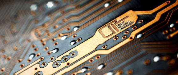
Copper Innovation Technologies New Flexible Copper-Clad Laminated Film (FCCL)

Copper Innovation Technologies (CIT, official site) is a company we’ve had an opportunity to talk to around the December to CES 2024 timeframe. They developed a new Copper-Clad Laminated Film (FCCL) technology to improve electronic data transmission by reducing the signal-to-noise ratio (SNR). The FCCL principle works as follow: a copper layer is somehow bonded to a flexible substrate (plastic-looking material). This enables the building of flexible printed circuit boards (PCB) with precise circuitry. In an era of flexible displays and foldable devices, you can imagine how valuable this technology can be for cutting-edge electronics. In addition to the flexible nature of its FCCL technology, CIT also points out that its copper material has a single-crystal structure, which means that atoms are exceptionally well aligned, with fewer grain boundaries. This structure allows for even better electric and thermal conductivity as grain boundaries impede the flow of electrons, thus maintaining signal integrity (noise reduction). The lower resistivity of this kind of copper is also crucial to transmitting a signal with minimal loss and interference. That’s particularly true for a weak original signal. The same properties can be significant for very high-speed signals such as 5G and 6G going forward. No matter the throughput, the technology that CIT is working on could drastically improve tomorrow’s electronic products. CIT started by researching how to deposit Copper on Teflon. Along the way, the company developed an innovative solution that could have broader application; that’s when the company was founded, and it is currently located in Busan, but plans to expand internationally. For example, the company can build cables with significantly reduced grain boundaries, which means they’ll introduce as little noise as possible for analog signals. Some signals are very faint in the medical field, and it is critical to transmit them without introducing noise. That’s true for every “measurement” application. CIT representatives said they intend to start addressing the electronics circuit market that uses Teflon, but plan to extend to more areas later. One of the goals is to increase the deposition area size, which can be addressed during manufacturing. Currently, 50x50cm is the near-term goal to reach mass production truly. If all goes well, CIT expects to address most markets, from audio to medical MRI products. Most consumers might never know who built some flexible boards inside their devices, but CIT might become a critical participant in that market in the coming years. Filed in Korea, Semiconductors and South Korea. . Read more about
