Highlights of the TSMC Open Innovation Platform Ecosystem Forum – Semiwiki

TSMC recently held their 10th annual Open Innovation Platform (OIP) Ecosystem forum. The talks included a technology and design enablement update from TSMC, as well as specific presentations from OIP partners on the results of recent collaborations with TSMC. This article summarizes the highlights of the TSMC keynote from L.C. Lu, TSMC Fellow and Vice-President, Design and Technology Platform, entitled: “TSMC and Its Ecosystem for Innovation”. Subsequent articles will delve more deeply into specific technical innovations presented at the forum.
TSMC OIP and Platform Background
Several years ago, TSMC defined four “platforms”, to provide specific process technology and IP development initiatives aligned with the unique requirements of the related applications. These platforms are:
L.C.’s keynote covered the recent advances in each of these areas.
OIP partners are associated with five different categories, as illustrated in the figure below.
EDA partners develop new tool features required to enable the silicon process and packaging technology advances. IP partners design, fabricate, and qualify additional telemetry, interface, clocking, and memory IP blocks, to complement the “foundation IP” provided by TSMC’s internal design teams (e.g., cell libraries, general purpose I/Os, bitcells). Cloud service providers offer secure computational resources for greater flexibility in managing the widely diverse workloads throughout product design, verification, implementation, release, and ongoing product engineering support. Design center alliance (DCA) partners offer a variety of design services to assist TSMC customers, while value chain aggregation (VCA) partners offer support for test, qualification, and product management tasks.
The list of OIP partners evolves over time – here is a link to an OIP membership snapshot from 2019. There have been quite a few recent acquisitions, which has trimmed the membership list. (Although not an official OIP category, one TSMC forum slide mentioned a distinct set of “3D Fabric” packaging support partners – perhaps this will emerge in the future.)
As an indication of the increasing importance of the OIP partner collaboration, TSMC indicated, “We are proactively engaging with partners much earlier and deeper (my emphasis) than ever before to address mounting design challenges at advanced technology nodes.”
Here are the highlights of L.C.’s presentation.
In previous technical conferences, TSMC indicated that there will be (concurrent) process development and foundation IP releases focused on the HPC platform for advanced nodes.
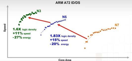
The figures below illustrate the PPA targets for the evolution of N7 to N5 to N3. To that roadmap, TSMC presented several design technology co-optimization (DTCO) approaches that have been pursued for the N3HPC variant. (As has been the norm, the implementation of an ARM core block is used as the reference for the PPA comparisons.)
Examples of the HPC initiatives include:
N3HPC cells adopt a taller image, enabling greater drive strength. Additionally, double-high cells were added to the library. (Complex cells often have an inefficient layout, if confined to a single cell-height image – although double-high cells have been used selectively in previous technologies, N3HPC adopts a more diverse library.)
Although perhaps counterintuitive, increasing the cell area may offer a performance boost by reducing the Cgs and Cgd parasitics between gate and S/D nodes, with M0 on top of the FinFET.
Traditionally, any “non-default rules” (NDRs) for metal wires were pre-defined by the PD engineer to the router (and often pre-routed manually); the EDA collaboration with TSMC extends this support to decisions made automatically during APR.
Note in the graph above that the improved N3HPC performance is associated with a slight power dissipation increase (at the same VDD).
N5 Automotive Design Enablement Platform (ADEP)
The requirements for the Automotive platform include a more demanding operating temperature range, and strict reliability measures over an extended product lifetime, including: device aging effects, thermal analysis including self-heating effects (SHE), and the impact of these effects on electromigration failure. The figure below illustrates the roadmap for adding automotive platform support for the N5 node.
Cell-aware internal fault models are included, with additional test pattern considerations to reduce DPPM defect escapes.
RF CMOS has emerged as a key technology for mobile applications. The figure below illustrates the process development roadmap for both the sub-6GHz and mmWave frequency applications. Although N16FFC remains the workhorse for RF applications, the N6RF offering for sub-6GHz will enable significant DC power reduction for LNAs, VCOs, and power amplifiers.
As for the Automotive platform, device aging and enhanced thermal analysis accuracy are critical.
N12e sub-Vt operation
A major initiative announced by L.C. related to the IoT platform. Specifically TSMC is providing sub-Vt enablement, reducing the operating supply voltage below device Vt levels.
Background – Near-Vt and Sub-Vt operation
For very low power operation, where the operating frequency requirements are relaxed (e.g., Hz to kHz), technologists have been pursuing aggressive reductions in VDD – recall that active power dissipation is dependent upon (VDD**2).
Reducing the supply to a “near-Vt” level drops the logic transition drive current significantly; again, the performance targets for a typical IoT application are low. Static CMOS logic gates function at near-Vt in a conventional manner, as the active devices (ultimately) operate in strong inversion. The figure below illustrates the (logarithmic) device current as a function of input voltage – note that sub-Vt operation implies that active devices will be operating in the “weak inversion” region.
Static, complementary CMOS gates will still operate correctly at sub-Vt levels, but the exponential nature of weak inversion currents introduces several new design considerations:
Conventional CMOS circuits adopt a (beta) ratio of Wp/Wn to result in suitable input noise rejection and balanced RDLY/FDLY delays. Commonly, this ratio is based on the strong inversion carrier mobility differences between nFET and pFET devices. Sub-Vt circuit operation depends upon weak inversion currents, and likely requires a different approach to nFET and pFET device sizing selections.
The dependence of the circuit behavior on weak inversion currents implies a much greater impact of (local and global) device process variation.
Conventionally, a high ratio of Ion/Ioff is available to CMOS circuit designers, where Ioff is the leakage current through inactive logic branches. In sub-Vt operation, Ion is drastically reduced; thus, the robustness of the circuit operation to non-active leakage current paths is less. High fan-in logic gates (with parallel leakage paths) are likely to be excluded.
In a similar manner, the leakage paths present in an SRAM array are a concern, both for active R/W cell operation and inactive cell stability (noise margins). In a typical 6T-SRAM bitcell, with multiple dotted cells on a bitline, leakage paths are present through the access transistors of inactive word line rows.
A read access (with pre-charged BL and BL_bar) depends on a large difference in current on the complementary bitlines through only the active word line row array locations. In sub-Vt operation, this current difference is reduced (and also subject to process variations, as SRAMs are often characterized to a high-sigma tail of the statistical distribution curve).
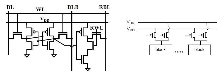
As a result, the number of dotted cells on a bitline would be extremely limited. The schematic on the left side of the figure below illustrates an example of a modified (larger) sub-Vt SRAM bitcell design, which isolates the read operation from the cell storage.

IoT applications may have very unique execution profiles. There are likely long periods of inactivity, with infrequent “burst mode” operations requiring high performance for a short period of time. In conventional CMOS applications, the burst mode duration is comparatively long, and a dynamic-voltage frequency-scaling (DVFS) approach is typically employed by directing a DC-to-DC voltage regulator to adjust its output. The time required for the regulator to adapt (and the related power dissipation associated with the limited regulator efficiency) are rather inconsequential for the extended duration of the typical computing application in burst mode.
Such is not the case for IoT burst computation, where power efficiency is utmost and the microseconds required for the regulator to switch is problematic. The right hand side of the figure above depicts an alternative design approach for sub-Vt IoT CMOS, where multiple supplies are distributed and switched locally using parallel “sleep FETs” to specific blocks. A higher VDD would be applied during burst mode, returning to the sub-Vt level during regular operation.
TSMC is targeting their initial sub-Vt support to the N12e process. The figure below highlights some of the enablement activities pursued to provide this option for the IoT platform.
TSMC hinted that the N22ULL process variant will also receive sub-Vt enablement in the near future.
L.C. also provided an update on the TSMC 3D Fabric advanced packaging offerings – look for a subsequent article to review these technologies in more detail.
TSMC provided several insights at the recent OIP Ecosystem forum:
and, perhaps the most disruptive update,
