On the Edge of Innovation: For the Present and the Future | NXP Semiconductors

Did you know that globally, data transmission networks consume
hundreds of terawatt hours (TWH), accounting for 1-2% of global electricity use? As mobile data transport requirements are still exponentially growing, the energy consumption associated with these networks is
becoming quite significant globally. Thus, efforts should be geared towards optimizing the performance of those mobile networks
and reducing the throughput requirements.
We don’t always realize the “hidden” cost associated with data transport to a centralized (cloud) location or the cost of data
storage. From an energy consumption standpoint, it can be helpful to skip data storage and/or communication cost to the cloud
network and instead process the data in-place. This allows for all kinds of physical locations to do data processing, from the
extreme edge (at the sensor), to the cloud and all locations in the middle. Multiple processes take place in between, beyond
cell local data to include IoT gateway, local data center, cell site and so on.
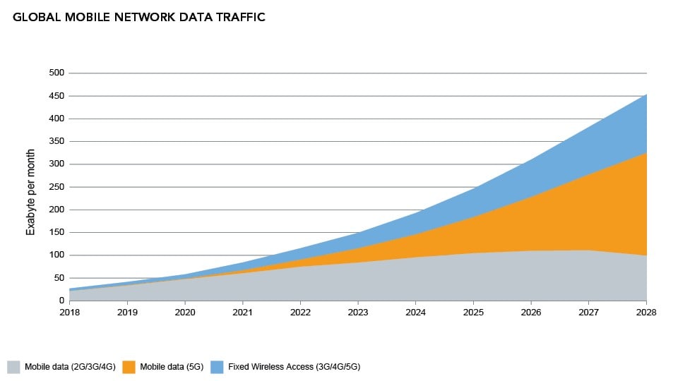
Figure 1 shows how data transmission (which is already consuming 1-2% of worldwide electricity consumption) continues to be on
an upward curve in the coming years. This means that communication and compute will become a bigger component of global
electricity use unless electricity cost is reduced drastically. This makes the case for more localized processing. Putting the
data processing at other locations optimizes aggregate use of energy — moving more and more systems to a “processing at the
edge” model. This edge processing comes with extra benefits such as increased privacy and data protection, but how can it become
a reality?
Overcoming the Challenges of Edge Processing
There’s more to energy frugality. Processing at the edge may be the right move, but there’s still a plethora of implementation options. It’s interesting
to observe how application mapping has become increasingly complex. It’s only a few decades ago when embedded microcontrollers
and processors alike consisted of a single processing unit (CPU) with with some associated I/O. In such an environment,
there’s little question on which algorithm works where: they all run on a single CPU. Things are different these days: a modern
embedded processor such as the
NXP i.MX product line
has CPUs, but also graphics processors (GPUs), neural processors (NPUs), signal processors (DSPs) and various hardware
accelerators. This makes for a fascinating exercise in mapping the application to the available silicon. Do I want to run my
algorithm on a CPU, GPU, NPU, DSP or accelerator? Note how the software complexity of the system goes up here.
Power optimization is another factor in designing and manufacturing devices for edge processing. This comes down to balancing
active power consumption. The active power is impacted of course by CPU frequency, but also workload, how the other accelerators
are being used, the amount of data going to/from external memory, the system components that are being used (e.g. display and
backlight), connectivity such as Wi-Fi, and the temperature of the environment, among others. Static power is going to be how
much of the die is powered up versus gated, meaning the process at which my processing unit executes.
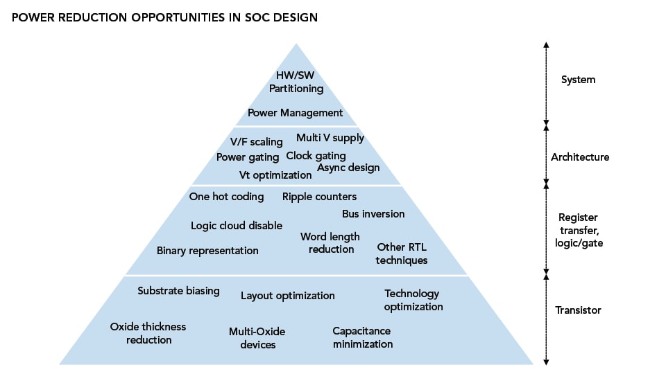
It’s crucial to explore and utilize further power reduction opportunities in SoC design. Power reduction at the edge implies
that the chips that are used at the edge need to be optimized for power consumption. This plot shows a wide range of mechanisms
that have been developed over time to improve power consumption from a silicon and system point of view.
Enhancing Power Measurement and Power Optimization Workflow
In practice, this emphasis on power consumption is a part of any good system and silicon design workflow. At NXP, in addition to
our unique SoCs, such as i.MX 7ULP and i.MX 8ULP that are optimized for power consumption, we’re optimizing the different power
modes on silicon in a use case environment. We have power app notes that detail the approaches which are reproducible with our
broad support package software (BSP SW) while the notes also provide useful guidance for our customers. Furthermore, our focus
extends to streamlining as much as possible the overall power management of the device from a system level via the co-design of
PMIC. We also implement the use of low-power DRAM (LP4, LP4X, LP5) to assist with system level power reduction – lower voltage
of operation and self-refresh modes in standby among others.
Bringing ultra-low power processing and advanced integrated security to the intelligent edge. Discover our
scalable and secure
i.MX 8ULP applications processors.
Saving Energy in Deployment and Life Cycle
There’s a lot of attention on device and system optimization which covers device architecture, design, manufacturing and system development to development to make a product. But many of today’s products are designed to have only a very limited lifetime in the
market. This causes a replacement cycle where consumers need to upgrade to new hardware every few years. This can be deemed
wasteful and represents an opportunity for improvement.
Beyond the physical device availability, the obvious answer is to use the increasing software-centricity of devices to extend
their life cycle as much as possible. Software upgradeability can be used to incrementally provide more features over time. This
allows the lifetime to be extended. What is needed to support this concept is a huge ecosystem that supports the security
requirements needed to ensure that only intended software is loaded on the device. This is another area where NXP has been
putting a lot of development effort.
Security and efficiency are vital in developing edge ML applications. Download NXP’s
Essentials of Edge Computing
to learn more.

Taking It Further – What Lies Ahead
This blog has explored a few aspects of sustainability from the chip industry’s point of view. First, it covered the
optimization of the communication network between the edge and the cloud. Second, SoC workload optimization of the chip and
associated system design. Lastly, it briefly touched on lifecycle management which is needed to ensure devices can stay in the
market longer.
Some aspects NXP is actively working on to achieve a greener world have been highlighted. However, cross-industry collaboration
is needed for all this to become more feasible. In the industry, most engineering time and effort are still focused on
short-term optimization to performance targets without optimizing explicitly for power or long-term sustainability. A mindset
change is needed to change this view.