TSMC OIP – Enabling System Innovation – Semiwiki

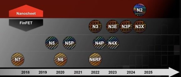
On November 10th I watched the presentation by L.C. Lu, TSMC Fellow & VP, as he talked about enabling system innovation with dozens of slides in just 26 minutes. TSMC is the number one semiconductor foundry in the world, and their Open Innovation Platform (OIP) events are popular and well attended as the process technology and IP offered are quite compelling to many semiconductor design segments. The TSMC technology roadmap showed a timeline of both FinFET and Nanosheet plans out through 2025.
Starting with N3 there’s something new called FinFlex that used Design Technology Co-Optimization (DTCO), promising an improved Power, Performance and Area (PPA) for segments like energy-efficient and high-performance. With the FinFlex approach a designer can choose from three transistor configurations, based on their design goals:
The history of fin block choices used in process nodes N16 to N3 are shown below:
EDA vendors Synopsys, Cadence, Siemens EDA and ANSYS have updated their tools to support FinFlex, and within a single SoC you can even mix the fin block choices. Along timing critical paths you can use high-fin cells, while non-critical path cells can be low fin. As an example of process scaling benefits, Lu showed an ARM Cortex-A72 CPU implemented in N7 with 2 fin, N5 with 2 fin, and finally N3E with 2-1 fin:
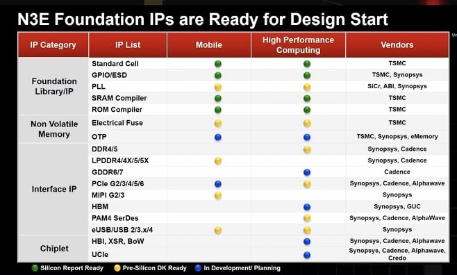
IP cells for N3E come from several vendors: TSMC, Synopsys, Silicon Creations, Analog Bits, eMemory, Cadence, Alphawave, GUC, Credo. There are three states of IP readiness: silicon report ready, pre-silicon design kit ready, and in development.
Analog IP
At TSMC their analog IP is using a more structured regular layout, which produces a higher yield and lets EDA tools automate the analog flow to improve productivity. The TSMC Analog Cell has a uniform poly and oxide density, helping with yield. Their analog migration flow, automatic transistor sizing and matching driven Place and Route enables design flow automation with Cadence and Synopsys tools.
Analog cells can be migrated through steps of: Schematic migration, circuit optimization, auto placement and auto routing. As an example, migrating a VCO cell from N4 to N3E using their analog migration flow took 20 days, versus a manual approach requiring 50 days, some 2.5X faster.
TSMC has three types of packaging to consider:
There are eight choices of packaging in 3DFabric:
A recent example using SoIC packaging was the AMD EPYC Processor, a data center CPU, which showed a 200X interconnect density improvement over 2D packaging, a 15X density improvement over traditional 3D stacking, producing a 50-80% better CPU performance.
3D IC design complexity is addressed through 3Dblox, a methodology using a generic language for EDA tool interoperability, covering the physical architecture and logic connectivity. The top four EDA vendors (Synopsys, Cadence, Siemens, Ansys) have readied their tools for the 3Dblox approach by completing a series of five test cases: CoWoS-S, InFO-3D, SoIC, CoWoS-L 1, CoWoS-L 2.
TSMC has created a 3DFabric alliance by collaborating with vendors across the realms of: IP, EDA, Design Center Alliance (DCA), Cloud, Value Chain Alliance (VCA), Memory, OSAT, Substrate, Testing. For memory integration TSMC partners with Micron, Samsung Memory and SK hynix, to enable CoWoS and HBM integration. EDA test vendors include: Cadence, Siemens EDA and Synopsys. IC test vendors include: Advantest and Teradyne.
